
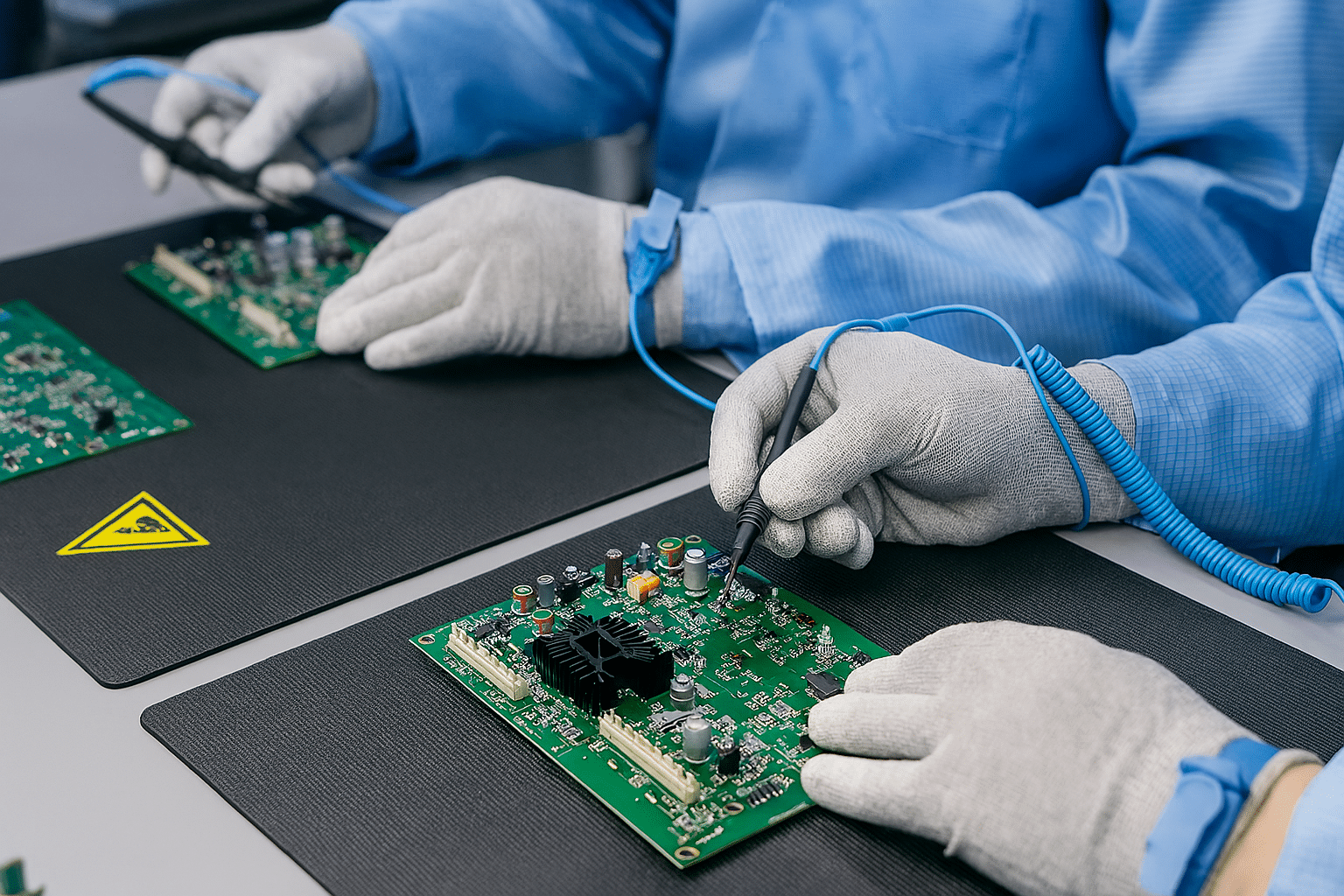
ESD, The Complete A-Z
Part 1: The Fundamentals
1.1 First: What exactly is ESD?
ESD = Electrostatic Discharge.
It is the sudden transfer of electrostatic charge between two objects at different electrical potentials.
The classic example:
We walk across a carpet. Our body accumulates charge. We touched a metal door handle. Zap. That tiny spark is ESD.
The same phenomenon happens inside factories—but instead of our finger getting a small shock the discharge can damage:
- semiconductor dies
- ICs
- MOSFETs
- sensors
- microcontrollers
- memory
- automotive electronics
- EV battery electronics
- aerospace electronics
- medical electronics
1.2 The fundamental concept
We need to understand five things before anything else:
| Concept | Definition | Unit |
|---|---|---|
| Charge | An object can have an excess or deficiency of electrons | Measured in coulombs (C) |
| Voltage | Voltage is an electric potential difference. It tells us how much potential exists between the two points | — |
| Current | Current is the movement of charge | Measured in amperes |
| Resistance | Resistance opposes current flow | Measured in ohms (Ω) |
| Capacitance | Capacitance describes an object's ability to store electrical charges | Measured in farads (F) |
These five concepts are the foundation.
1.3 Where does static electricity come from?
The biggest mechanism we need to learn is: Triboelectric charging
Two materials come into contact and then separate. During that process, the charge can be transferred.
Examples:
- shoes + floor
- plastic + plastic
- tape + surface
- gloves + components
- packaging + IC
- clothing + chair
- conveyor belt + product
Part 2: The Human Factor
2.1 Why humans are dangerous
The human body is basically a capacitor.
Imagine:
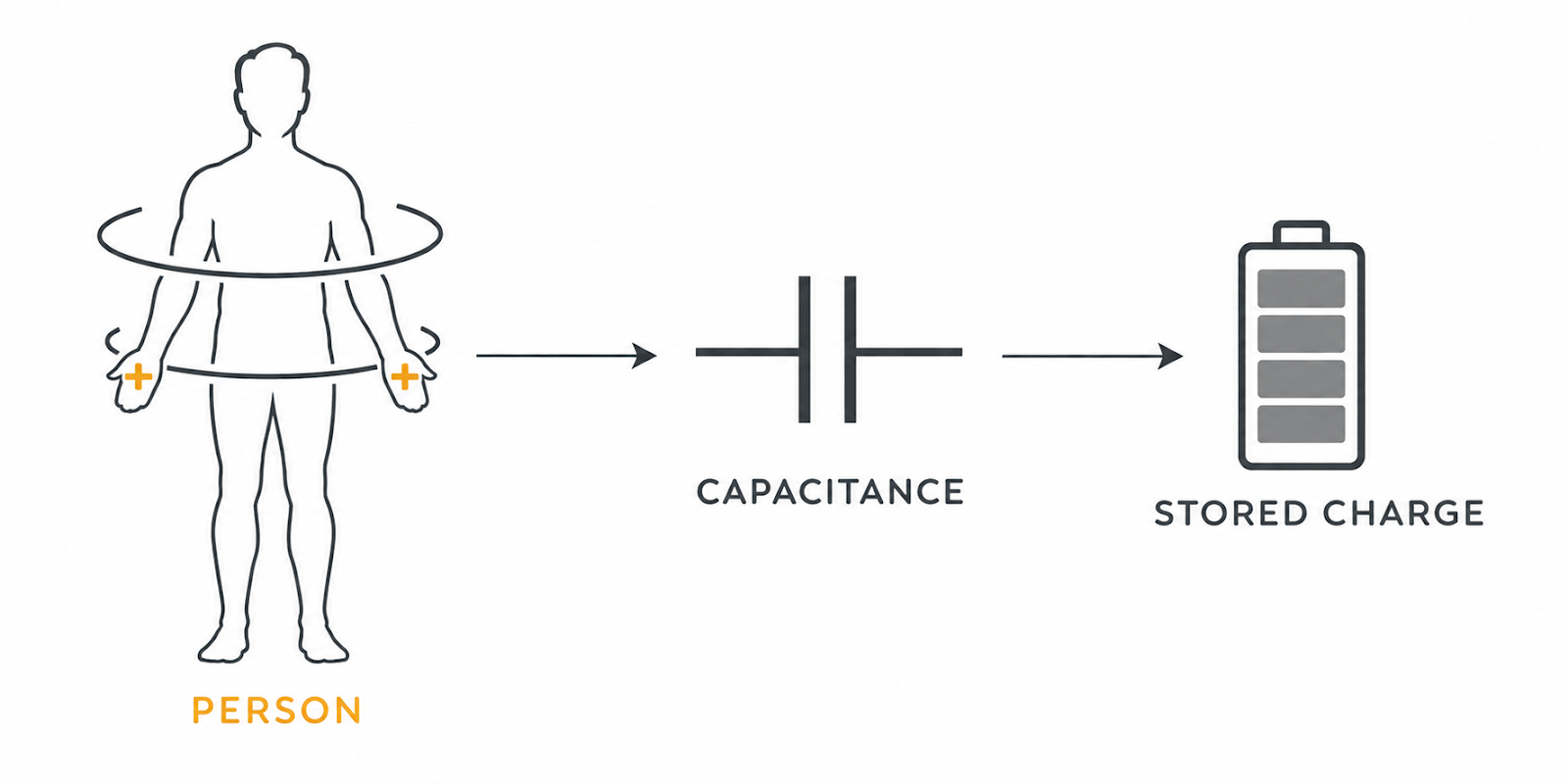
A person can accumulate substantial electrostatic potential simply by:
- walking
- moving
- removing clothing
- handling plastic
- sitting on chairs
- moving across floors
2.2 The dangerous misconception
A beginner thinks: "If I don't feel the shock, there is no ESD."
Wrong.
Humans typically don't perceive many electrostatic events that can still damage sensitive electronics.
An ESD event can be: fast + high current + extremely short duration.
So ESD isn't primarily about whether humans feel something. It's about what the electronic device experiences.
Part 3: Damage and Risk
3.1 The three major ESD mechanisms
We need to master these things.
| Model | What it represents |
|---|---|
| Human Body Model — HBM | Represents a charged human touching device. Important in semiconductor device testing. |
| Charged Device Model — CDM | The device itself becomes charged and then discharges. This is especially important in modern semiconductor manufacturing because components can be extremely sensitive. |
| Machine Model — MM | Historically represented discharge from a charged machine/tool. We'll encounter MM in ESD literature, although modern semiconductor qualification has moved away from using MM as a primary component qualification model. |
3.2 ESD damage
There are two major categories.
3.2.1 Catastrophic failure
The component dies immediately.
Example:
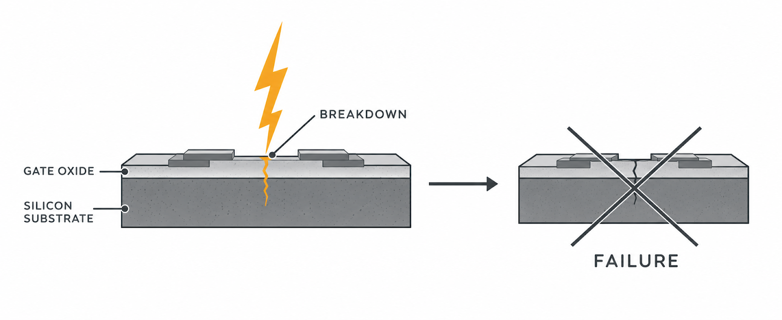
Easy to detect.
3.2.2 Latent failure
This is much more dangerous commercially. The ESD event damages the component but doesn't immediately kill it. The product passes testing. Then:
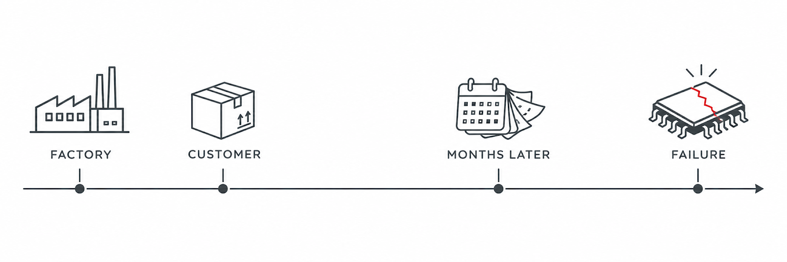
Now the manufacturer has:
- warranty costs
- field failures
- recalls
- reputation damage
- lost customers
3.3 ESD doesn't only damage electronics
ESD can also cause:
Ignition
In environments containing flammable materials, an electrostatic spark can ignite vapors, gases or dust.
Contamination
Electrostatic fields can attract particles.
Process problems
Static can cause:
- films to stick
- components to move
- dust attraction
- robotic handling problems
- material feeding problems
Part 4: ESD Control Philosophy
4.1 The ESD Protected Area
We will hear: EPA — ESD Protected Area.
This is the controlled environment where ESD-sensitive devices are handled.
A proper EPA can include:
- ESD flooring
- personnel grounding
- ESD workstations
- conductive/dissipative surfaces
- grounding systems
- ionization
- ESD garments
- controlled packaging
- signage
- procedures
- training
- audits
- verification
4.2 The ESD control philosophy
Here's the fundamental idea: Don't allow uncontrolled charges to accumulate, and don't allow uncontrolled discharge to reach the sensitive device.
We achieve that through:
| Method | Purpose |
|---|---|
| Grounding | Give charge a controlled path to earth/reference |
| Bonding | Connect conductive objects so they are at approximately the same electrical potential |
| Dissipation | Allow charges to move away in a controlled manner |
| Shielding | Protect sensitive devices from external electrostatic fields/discharges |
| Ionization | Neutralize charge on otherwise isolated objects |
| Packaging | Keep ESD-sensitive devices protected during transportation/storage/handling |
4.3 Conductive vs dissipative vs insulative
This is critical. We need to understand the resistance ranges and more importantly, the terminology used by the applicable standard/test method.
Broadly:
| Category | Resistance | Behaviour |
|---|---|---|
| Conductive | Low resistance | The charge moves relatively easily |
| Dissipative | — | Charge moves more slowly and controllably. This is extremely important for ESD work surfaces and flooring |
| Insulative | High resistance | Charge does not readily move through the material |
Static dissipative ≠ conductive
A beginner often thinks: "More conductive = better ESD." Not necessarily. We don't simply want electricity to rush through everything. We want controlled charge dissipation appropriate to the application.
Part 5: Putting Control Into Practice
5.1 The ESD control triangle
Think about:
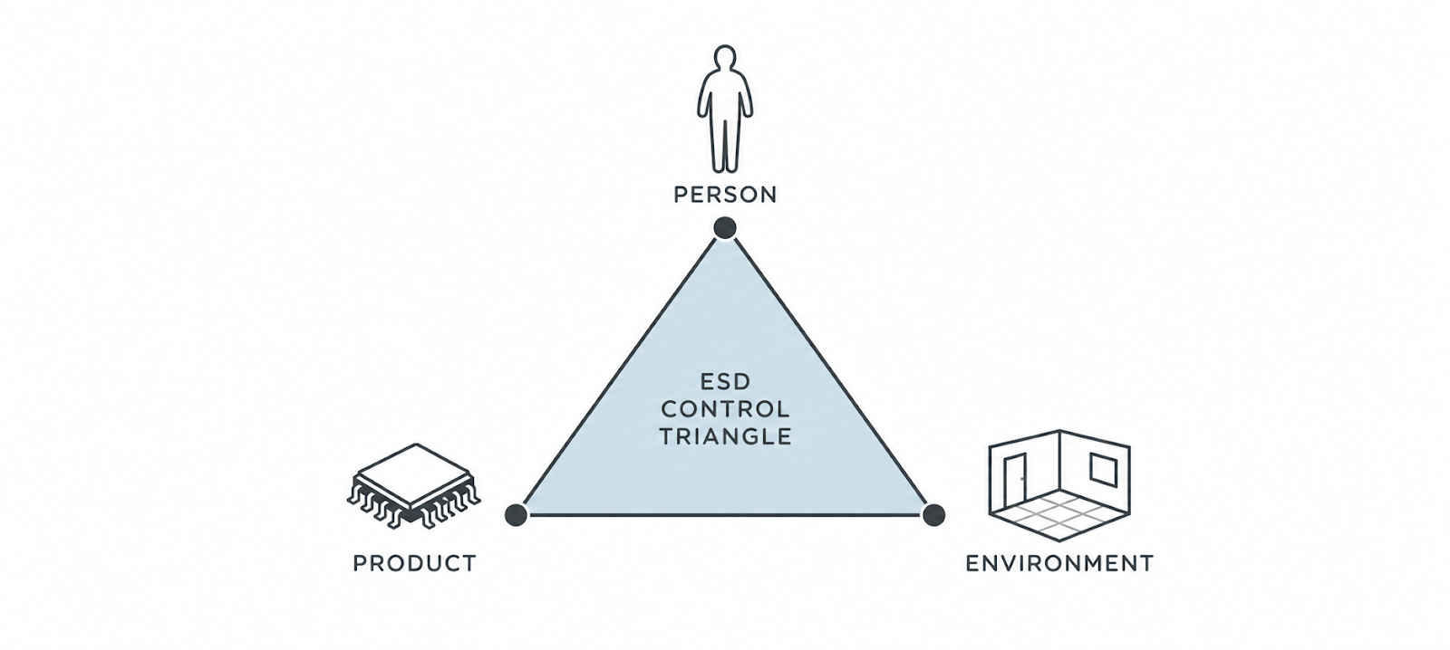
We need to control all three.
Person
- wrist strap
- footwear
- garments
- grounding
- training
- ESD packaging
- trays
- bags
- containers
- shielding
- floor
- workstation
- grounding
- humidity
- ionizers
- equipment
5.2 ESD flooring
A major commercial category.
Typical systems include:
- ESD vinyl
- conductive vinyl
- dissipative epoxy
- conductive epoxy
- ESD rubber
- specialty tiles
We need to consider:
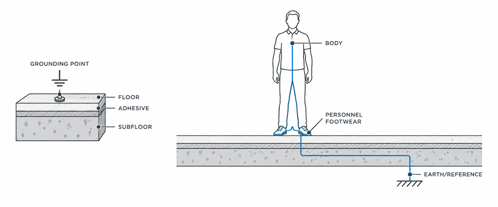
The entire system matters.
5.3 ESD workstation
A proper workstation may contain:
- ESD workbench
- dissipative work surface
- grounding point
- wrist strap connection
- common point ground
- shelving
- ESD chair
- ionizer
- ESD tools
- ESD lighting
- ESD storage
5.4 Wrist straps
A wrist strap provides a controlled path between the operator and the grounding system.
But: wrist strap alone ≠ ESD program.
We need:
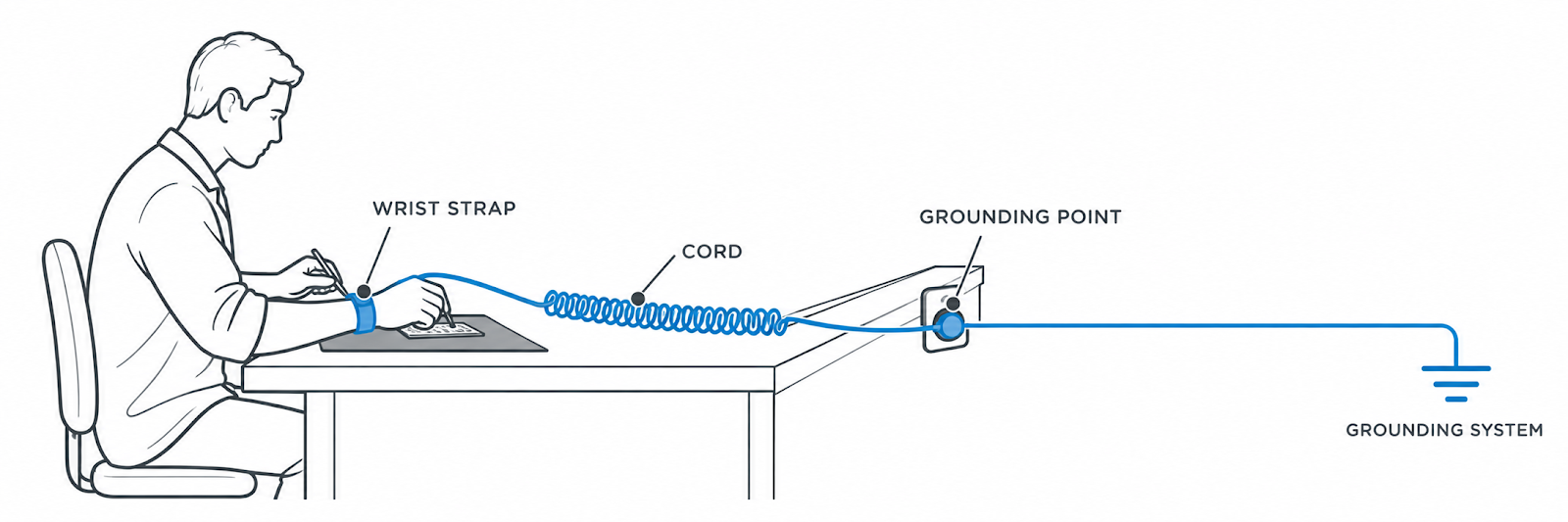
And that system needs verification.
5.5 ESD footwear
Instead of grounding through the wrist, personnel can use:
- ESD shoes
- heel grounders
- toe grounders
- conductive footwear
5.6 Ionizers
Here's where things get interesting.
Some objects cannot easily be grounded.
For example: plastic component
It's an insulator. We can't simply attach a ground wire and expect the charge to disappear.
So, we use: Ionization
An ionizer generates positive and negative ions. These neutralize electrostatic charges.
We'll find ionizers in:
- semiconductor assembly
- SMT lines
- cleanrooms
- laboratories
- electronics manufacturing
- packaging areas
5.7 ESD packaging
This is a HUGE industry.
Think:
5.7.1 Primary packaging
Directly protects the component.
Examples:
- bags
- trays
- tubes
- carriers
5.7.2 Secondary packaging
Protects groups of components.
Examples:
- boxes
- totes
- containers
5.7.3 Shielding packaging
Designed to provide protection from electrostatic fields/discharge.
Examples:
- shielding bags
- shielding containers
5.8 ESD polymers
Normal plastic: highly insulating
ESD plastic: engineered electrical behavior
We can modify polymers using:
- antistatic additives
- conductive fillers
- carbon-based materials
- conductive fibers
- polymeric dissipative systems
- specialty additives
electrical resistance + mechanical properties + processing + durability + contamination + cost + environmental stability
That is a material engineering problem.
5.9 Why ESD polymers are difficult
Suppose we manufacture an ESD tray. We need:
- correct resistance
- dimensional stability
- impact resistance
- temperature resistance
- chemical resistance
- low particle generation
- repeatable formulation
- consistent batch properties
- injection-molding compatibility
- long-term ESD performance
- humidity
- temperature
- additive migration
- wear
- contamination
- processing conditions
Part 6: Standards, Testing, and Industry
6.1 Standards — This is how KOLDPWR works?
We need to know the major standards of the ecosystem. The two most important ones we'll encounter are:
ANSI/ESD S20.20
A major ESD control program standard. It addresses establishing, implementing and maintaining an ESD control program.
IEC 61340-5-1
International standard for protection of electronic devices from electrostatic phenomena.
We should eventually know these standards deeply not just their names. Also learn the relevant test methods and product-specific standards around:
- resistance
- footwear
- flooring
- packaging
- ionization
- personnel grounding
- ESD protective equipment
- component sensitivity
6.2 ESD Association
We should become extremely familiar with the ESD Association (ESDA). It is one of the major organizations in the ESD field.
We should study:
- standards
- technical reports
- training
- certification
- ESD program requirements
- test methods
- industry terminology
6.3 IEC
The International Electrotechnical Commission is another major standards body. IEC 61340 is particularly important for international ambitions.
6.4 ESD testing
We need to know how to measure ESD performance. Important concepts include:
| Measurement | What it tells you |
|---|---|
| Resistance-to-ground | How easily the charge can flow from a surface/person to ground |
| Point-to-point resistance | Resistance between two points on a surface |
| Surface resistance | Electrical resistance across a material's surface |
| Charge decay | How quickly charge disappears |
| Static field measurement | Measurement of electrostatic fields |
| Ionizer performance | Things such as: offset voltage, discharge/decay time |
These are practical ESD engineering measurements.
6.5 KOLDPWR ESD laboratory
We have equipment such as:
- resistance meters
- surface resistance electrodes
- megohmmeters
- charge plate monitors
- electrostatic field meters
- wrist-strap testers
- footwear testers
- ionizer test equipment
- environmental chamber
- temperature/humidity monitoring
- ESD event generators
- specialized packaging test equipment
6.6 ESD audit
This connects directly to our earlier KOLDPWR plan. We entered a factory. We don't just look around. We systematically assess:
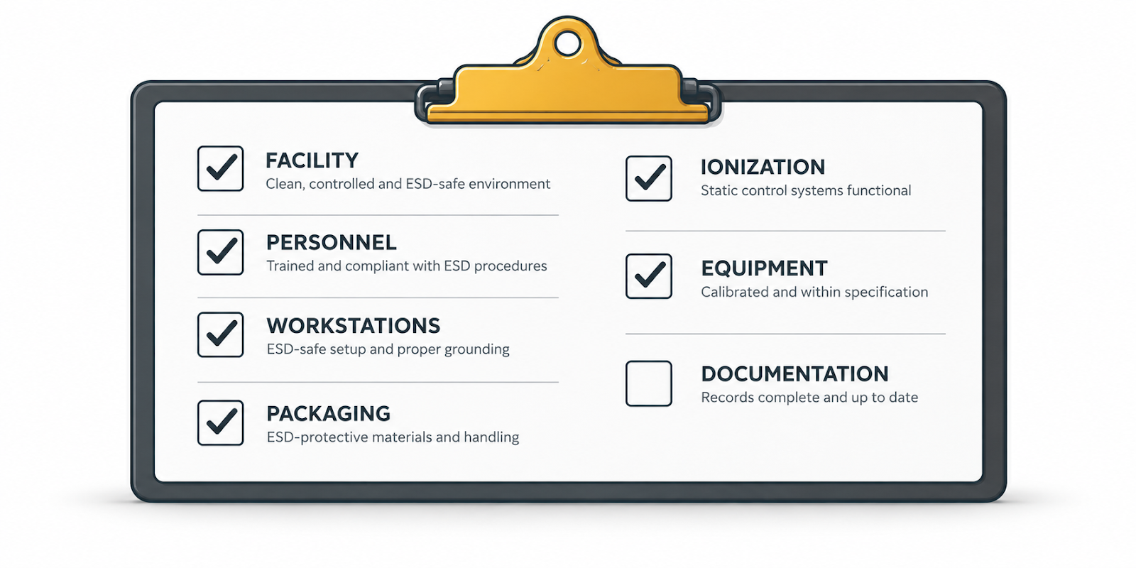
Then:
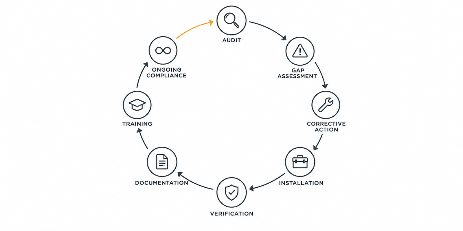
THAT IS WHY KOLDPWR MATTERS
6.7 ESD certification
We need to distinguish between: company/facility ESD program certification and individual ESD competency/training.
For example, an organization may implement an ESD control program against a recognized standard and undergo certification/assessment through an appropriate certification body.
We should eventually understand:
- certification
- registration
- accreditation
- laboratory accreditation
- auditor qualifications
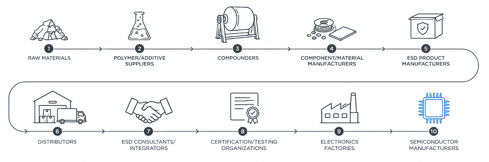
6.8 The ESD supply chain
Now zoom out. The global ESD industry includes:
Part 7: Industries and Sectors
7.1 Industries that need ESD
| Industry | Examples |
|---|---|
| Semiconductor | fabs, OSAT, semiconductor assembly, testing, packaging |
| Electronics | PCB assembly, SMT, EMS, electronics manufacturing |
| EV | battery cells, battery packs, BMS, power electronics, inverters, chargers, motor controllers |
| Automotive | ECUs, sensors, ADAS, radar, infotainment |
| Aerospace | avionics, satellites, spacecraft electronics |
| Defense | electronics, radar, communication systems |
| Medical | diagnostic equipment, implants, electronic medical devices |
| Optoelectronics | LEDs, lasers, optical sensors |
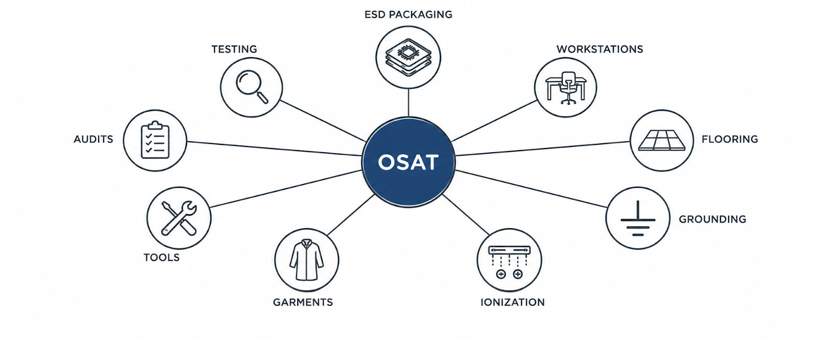
7.2 OSAT
We asked this earlier. OSAT = Outsourced Semiconductor Assembly and Test. The ecosystem can require:
7.3 Semiconductor fabs
This is the extreme end of the ESD world. A semiconductor fab has:
- cleanrooms
- sophisticated equipment
- highly controlled environments
- extremely sensitive devices
- strict contamination control
- advanced ESD controls
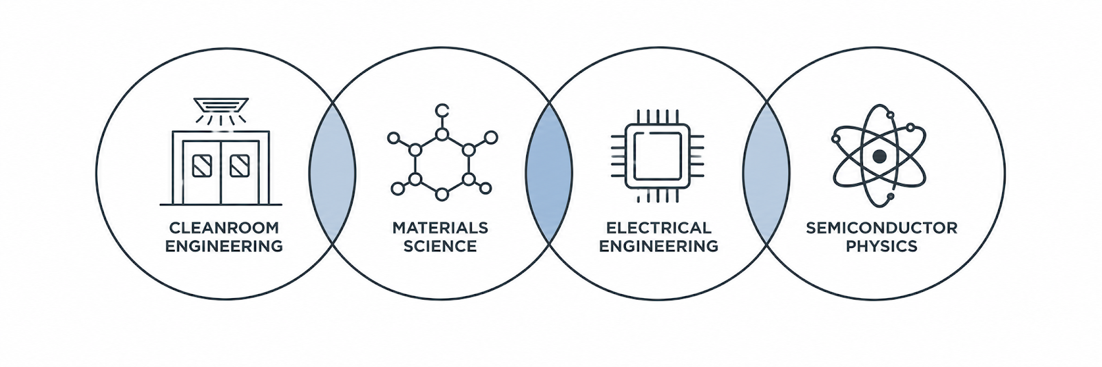
7.4 ESD + cleanrooms
This is a particularly important intersection. We can't simply introduce any ESD material into a cleanroom. We may need to consider:
- particle generation
- outgassing
- contamination
- ionic contamination
- chemical compatibility
- cleanability
- wear
- static charge
7.5 ESD + EV
Modern EVs contain huge amounts of electronics. Think:
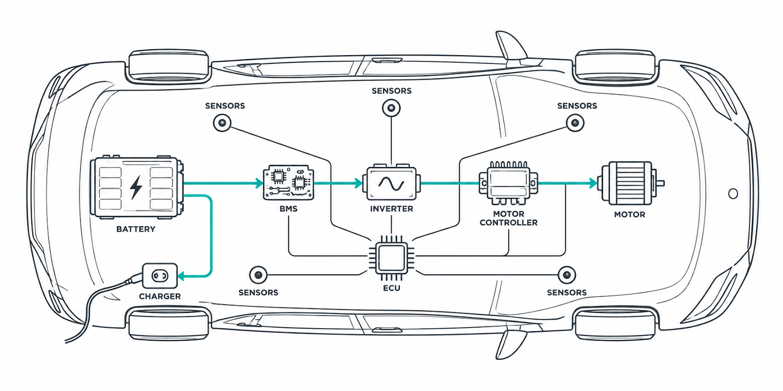
Many electronic components are ESD sensitive.
And lithium-ion battery manufacturing introduces additional electrostatic considerations because static charge can interact with:
- powders
- films
- separators
- dust
- production equipment
- electronic monitoring systems
7.6 ESD + semiconductor manufacturing in India
This could become strategically important. India is developing capabilities across:
- semiconductor assembly
- testing
- packaging
- electronics manufacturing
- semiconductor supply chains
Part 8: The History of Static Electricity
8.1 The history — how humans discovered static electricity
Now let's go back thousands of years.
Ancient Greek observers noticed something fascinating: Amber rubbed with certain materials could attract lightweight objects.
The Greek word associated with amber is: ēlektron
That's one origin of the word electricity.
For centuries, people observed electrostatic effects without understanding what was happening.
8.2 William Gilbert
In the late 1500s/early 1600s, William Gilbert systematically studied magnetic and electrical phenomena.
He helped establish the distinction between magnetic effects and what we now call electrical effects. This was an important step toward modern electricity.
8.3 Benjamin Franklin
Franklin famously studied electricity and helped establish the idea of electrical charge. His work contributed to the understanding of:
- positive and negative charge
- electrical phenomena
- lightning
8.4 Coulomb
Charles-Augustin de Coulomb established the relationship between electric force and charge. This eventually gave us Coulomb's law.
The force between charges depends on:

We need to understand what it means physically.
8.5 Faraday
Michael Faraday transformed our understanding of:
- electric fields
- electromagnetic induction
- capacitance
- electrostatics
8.6 Maxwell
James Clerk Maxwell unified electricity and magnetism mathematically. Eventually:
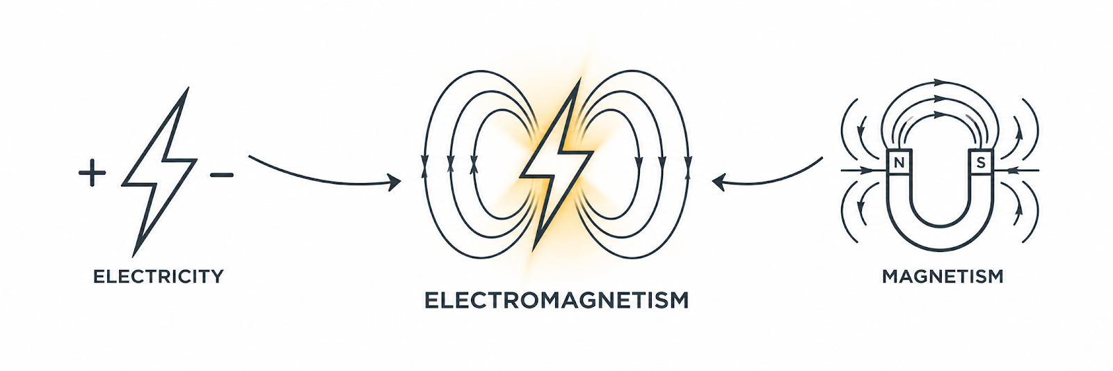
And ESD exists within that broader electromagnetic framework.
8.7 From physics to industrial ESD control
The problem changed dramatically with the invention of modern electronics. Early electronics were relatively robust. Then came:
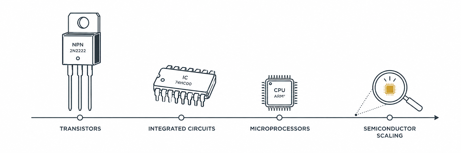
As devices became smaller, their structures became increasingly vulnerable to electrical overstress.
Suddenly: A tiny electrostatic discharge that a human barely notices could damage an expensive semiconductor.
That's when industrial ESD control became increasingly important.
8.8 Modern ESD engineering
Today ESD isn't simply: "Don't touch the circuit."
It's a complete engineering discipline involving:
- Physics
- Materials science
- Electrical engineering
- Semiconductor physics
- Manufacturing engineering
- Cleanroom engineering
- Quality management
- Testing
- Standards
- Supply chain